Digital Inputs
The regulator has two different styles of digital input architectures, depending on the pin in question. They are all exposed in the Ethernet Connectors (see Data Cables & Pinout).
- Optocoupler Style — Activated by a positive voltage input (rated 5–28 V applied to the input pin; survives to 54 V)
- Ground Style — Activated by shorting the input pin to ground
The two styles serve different installation scenarios: opto-style inputs are right for signals coming from elsewhere in the boat's 12/24/48 V system (ignition, BMS contacts, mode-switch outputs), where galvanic isolation matters and the signal source already has its own ground reference. Ground-style inputs are right for local switches mounted near the regulator that simply close to its own GND — they consume less idle power, eliminate the optocoupler aging concern, and are appropriate when the signal source is electrically local.
Optocoupler Channel Map (5 channels)
| Function | Opto IC | Series Diode | ESP32 GPIO |
|---|---|---|---|
| IGNITION (engine wake) | U5 | D19 | GPIO1 |
| HIGH/LOW (charging mode) | U10 | D25 | GPIO39 |
| BMSLogic (BMS enable) | U16 | D27 | GPIO42 |
| FORCEFLOAT (force float mode) | U17 | D28 | GPIO40 |
| EXTRA_OPTICAL_GPIO1 (spare) | U26 | D34 | GPIO8 |
All five channels are identical optically and electrically — only the destination GPIO differs. The V9 schematic below shows one real channel (U26, the spare EXTRA_OPTICAL_GPIO1 input); substitute the relevant designators from the table above for any other channel.
Note (audit 2026-05-23): U1 in the V9 schematic is the LSM6DSOX IMU — see LSM6DSOX IMU. The optocouplers are U5/U10/U16/U17/U26.
Optocoupler Style Digital Inputs
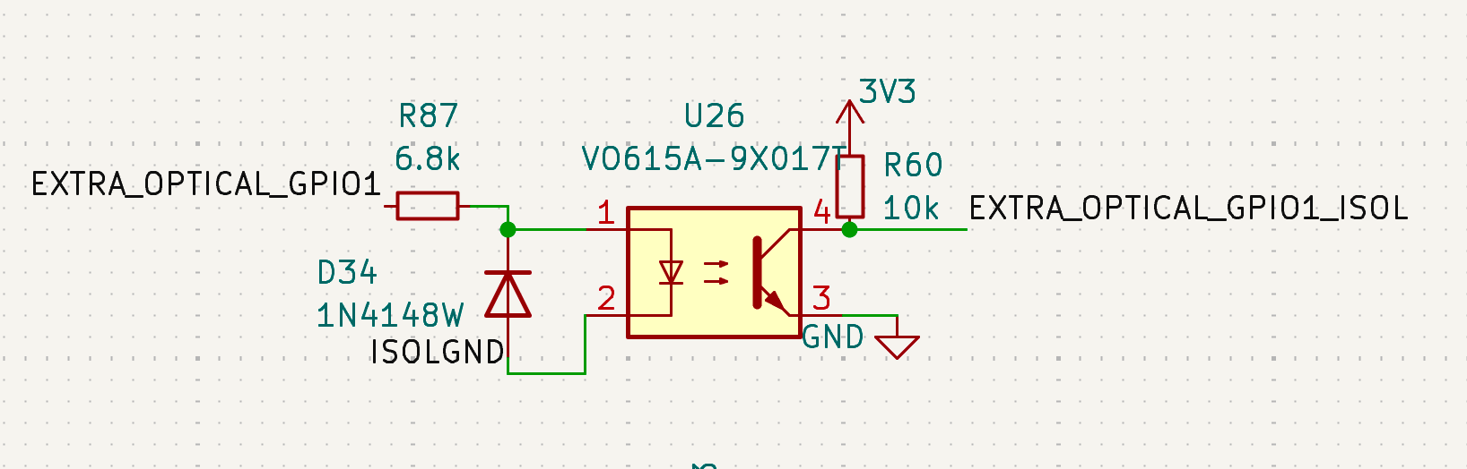
The input side (left, ISOLGND reference) takes the external 5–28 V signal through the 6.8 kΩ series resistor; the output side (right) is the isolated phototransistor pulling the ESP32 GPIO low against the 10 kΩ pull-up to 3.3 V.
Design Requirements
- Input voltage range: the published user-facing rating is 5–28 V (this keeps LED current in the 10+ year lifetime zone — see the table below). The circuit itself survives to 54 V with reduced LED lifetime.
- Temperature range: -40°F to 180°F (-40°C to 82°C) — well inside the VO615A's -55 °C to +110 °C rating
- Lifetime target: 10+ years at typical voltages (~12V), 3-6 years at the 54V survival limit
How an Optocoupler Works
The VO615A optocoupler provides electrical isolation between input circuit and ESP32 GPIO using light transmission:
Input Side (LED)
- Input voltage applied across current limiting resistor and IR LED
- Forward current flows through LED, producing infrared light
- Light intensity proportional to forward current
Output (ESP32 GPIO) Side (Phototransistor)
- IR light strikes phototransistor base region
- Light creates electron-hole pairs, acting as base current
- Transistor turns on, allowing collector current to flow
- Collector current = LED current × CTR (Current Transfer Ratio)
- When sufficient collector current flows, voltage at collector drops low enough to register as logic LOW on ESP32
- Voltage otherwise pulled high (3.3V) by pull up resistor to 3.3V Supply
Isolation Benefits
- Protection: High voltage transients on input side cannot damage ESP32
- Flexibility: Can accept input signals from 5V to 60V (lower life at higher voltages)
Component Selection
Optocoupler: VO615A-9X017T (LCSC C145478)
Decoding the part number against the datasheet's ordering-information table:
- -9 — CTR bin 9: 200–400 %, specified at IF = 5 mA, VCE = 5 V. (The unbinned base VO615A spans 50–600 % at the same test point.)
- X017T — SMD-4, package option 7, from the VDE-approved block (the "1" = option 1, DIN EN 60747-5-5 / VDE 0884-5); T = tape and reel.
- Agency approvals: UL 1577 / cUL, BSI, FIMKO, CQC, plus VDE with option 1.
Reason for the high-CTR bin: reliable switching at the 5 V low end, minimal extra cost.
CTR is specified at 5 mA — not at our low-end operating point
The 200–400 % bin is measured at IF = 5 mA. CTR falls off at lower LED current, so at the 5 V input level (IF ≈ 0.53 mA) the effective CTR is well below 200 %. The low-end analysis below therefore checks against the pull-up threshold current, not against the headline CTR number.
Current Limiting Resistor: 6.8kΩ, 1W, 2512 SMD
- Calculation basis:
- At 5V: IF = (5V - 1.43V) / 6.8kΩ = 0.53 mA
- At 54V: IF = (54V - 1.43V) / 6.8kΩ = 7.7 mA
- Power rating: 404mW at 54V requires 1W resistor for safety margin
Pull-up Resistor: 10kΩ, 0603 SMD (R60 shown for the U26 channel)
- Logic HIGH: When LED is OFF, phototransistor is OFF, collector pulled to 3.3V through 10kΩ
- Logic LOW: When LED is ON, phototransistor conducts, pulling collector toward ground
- Threshold current: the phototransistor must sink 3.3 V / 10 kΩ = 0.33 mA to pull the collector fully low
- Switching threshold: ESP32 typically switches at ~1.65V (50% of 3.3V), so even ~0.17 mA of collector current crosses the logic threshold
Performance Analysis
| Input Voltage | LED Current | vs Min (1mA) | Lifetime | Power (Watts) | Power (mA@12V) |
|---|---|---|---|---|---|
| 5V | 0.53 mA | 53% of min | 20+ years | 1.9 mW | 0.16 mA |
| 12V | 1.57 mA | 157% of min | 20+ years | 17 mW | 1.4 mA |
| 28V | 3.91 mA | 391% of min | 10+ years | 104 mW | 8.7 mA |
| 54V | 7.7 mA | 770% of min | 3-6 years | 404 mW | 33.7 mA |
Power consumption notes: - Power is consumed only when Input Signal is active (ie external switch is ON) - No power consumption when Input Signal = 0V (ie external switch OFF) - LED power = Forward current × 1.43V (LED forward voltage) - Resistor power = Forward current² × 6.8kΩ
Protection Diode: 1N4148W (SOD-123)
Function: Reverse Voltage Protection
The 1N4148W diode (SOD-123 package, LCSC C81598 — V9 BOM lists one per opto channel at D19, D25, D27, D28, D34) provides critical protection for the optocoupler LED:
- Normal operation: Diode is reverse biased across LED, no current flows
- Reverse voltage protection: If Input Signal goes negative, diode conducts and clamps reverse voltage to ~0.7V
- Prevents LED damage: VO615A LED can only handle 6V reverse voltage maximum
Why Critical
- Load dump transients: Long wires / disconnection can create voltage spikes
- Electrical noise: Marine electrical systems are electrically noisy environments
Specifications & Failure Limits
- Forward voltage: 0.7V typical, 1.25V maximum at 10mA
- Reverse voltage rating: 75V maximum
- Forward current rating: 300mA continuous, 2A peak (1µs pulse)
- Power dissipation: 350mW at 25°C
Failure Analysis
The diode will fail if: - Forward current > 300mA continuous: At maximum negative transient - Reverse voltage > 75V: If positive Input Signal exceeds 75V (well above our 54-60V max) - Power dissipation > 350mW: P = If × 0.7V, so fails at If > 500mA
The 1N4148WSX provides robust protection for all expected marine transient conditions.
System Power Consumption
| Condition | LED Side | ESP32 Side | Total Power | Total (mA@12V) |
|---|---|---|---|---|
| Input OFF | 0 mW | ~0 mW | ~0 mW | ~0 mA |
| Input ON (12V) | 17 mW | 1.09 mW | 18 mW | 1.5 mA |
| Input ON (54V) | 404 mW | 1.09 mW | 405 mW | 33.8 mA |
The ESP32-side 1.09 mW is the 10 kΩ pull-up conducting to ground through the phototransistor (3.3 V² / 10 kΩ) — it flows only while the input is active. With the input off, the phototransistor is off and the collector node is high-impedance, so the pull-up sources nothing: an idle opto channel consumes zero power on both sides.
LED Current Guidelines
- 1-3mA: Conservative operation (20+ year lifetime)
- 3-8mA: Moderate operation (5-10 year lifetime)
- 8-15mA: Aggressive operation (1-5 year lifetime)
Design Validation
- 5V switching: at 5 V the LED runs ≈ 0.53 mA. Even with CTR derated well below the 5 mA-spec 200 % floor, the phototransistor only has to sink 0.33 mA (the 10 kΩ pull-up's full-swing current) — and only ~0.17 mA to cross the ESP32 logic threshold — so switching remains reliable at the bottom of the range
- 54V survival: 7.7mA current provides marginal 3-6 year life if 100% duty cycle
- Temperature performance: VO615A-9's high CTR provides margin for temperature derating across -40°F to 180°F range
Bill of Materials (Optocoupler Style — per channel)
| Reference (per channel) | Part Number | Description | Package | LCSC |
|---|---|---|---|---|
| U5 / U10 / U16 / U17 / U26 | VO615A-9X017T | Optocoupler, CTR 200–400 % | SMDIP-4 | C145478 |
| R65 / R74 / R75 / R67 / R76 / R87 (6.8 kΩ pool) | — | Current-limit resistor, 1 W | 2512 | C26073 |
| R60 (10 kΩ pool — one per channel) | — | Pull-up resistor to 3V3 | 0603 | — |
| D19 / D25 / D27 / D28 / D34 | 1N4148W | Reverse-bias protection diode | SOD-123 | C81598 |
The 6.8 kΩ resistor pool (R65–R87 range) is shared across all five opto LED-drive series-resistors plus the buzzer-circuit gate pull-up (R65). The output pull-ups (R60 shown for the U26 channel) come from the board-wide shared 10 kΩ pool.
Ground Style Digital Inputs
Schematic
3.3V ──[10kΩ]──┬──[C51:1µF]──GND
               │
               ├──[D32:ESD]──GND
               │
               ├── Output Signal to ESP32 GPIO
               │
               └──[R5:500Ω]── Input Signal
Design Requirements
- Input method: Short to ground activation
- Temperature range: -40°F to 180°F (-40°C to 82°C)
- Debouncing: Hardware RC filter for switch bounce elimination
- Protection: ESD protection for exposed inputs
How Ground Style Inputs Work
This design uses RC debounce filtering:
Normal Operation (Switch Open)
- Input Signal is not connected (floating or open)
- No current flows to Ground
- Pull-up resistor R57 (10kΩ) pulls GPIO pin to 3.3V
- ESP32 GPIO reads logic HIGH (3.3V)
Activated Operation (Switch Closed to Ground)
- Input Signal is shorted to ground by external switch/contact
- Current flows from 3.3V through R57 (10kΩ) to ground via the switch
- Junction voltage: V_out = 0V (direct connection to ground)
- ESP32 GPIO reads logic LOW (0V << 0.8V threshold)
Component Analysis
Pull-up Resistor: R57 (10kΩ)
- Function: Pulls Output Signal HIGH when Input Signal is not grounded
- Power when input open: ~0 mW — the switch is open and the GPIO input is high-impedance, so the pull-up has no current path
- Power when input grounded: P = 3.3V²/10kΩ = 1.089 mW (continuous while held closed)
Debounce Capacitor: C51 (1µF)
- Function: Filters switch bounce and electrical noise
- Time constant: τ = R57 × C51 = 10kΩ × 1µF = 10ms
- Settling time: ~3τ = 30ms for clean switching
- Noise immunity: Filters high-frequency electrical noise
ESD Protection Diode: D32 (ESD5Z25.0T1G)
- Function: Clamps overvoltage transients to protect ESP32 GPIO
- Clamp voltage: 25V typical
- Application: Protects against static discharge and voltage spikes on input wiring
Performance Analysis
Switching Characteristics
- Rise time: Limited by RC time constant = 10ms
- Fall time: Much faster, limited by R5 and ESP32 input capacitance
- Debounce time: ~30ms eliminates typical switch bounce
Power Consumption
| Condition | Current | Power | Power (mA@12V) |
|---|---|---|---|
| Input Open | ~0 mA | ~0 mW | ~0 mA |
| Input Grounded | 0.33 mA | 1.089 mW | 0.09 mA |
Power consumption notes: - Power flows only while the switch is held closed — an open input draws nothing (high-impedance GPIO leaves the pull-up with no current path) - Very low power consumption suitable for battery applications - Worst case (switch held closed continuously) is still only ~1.1 mW
Voltage Levels
- Logic HIGH: 3.3V (input open/floating)
- Logic LOW: 0.157V (input grounded via voltage divider)
- Switching threshold: ESP32 switches at ~0.8V, providing excellent noise margin
- Noise margin HIGH: 3.3V - 0.8V = 2.5V
- Noise margin LOW: 0.8V - 0.157V = 0.64V
ESP32-S3 Internal ESD Protection and Real ESD Event Analysis
ESP32-S3 Internal Protection Specifications
From the ESP32-S3 datasheet:
- Human Body Model (HBM) ESD tolerance: ±2000V
- Charged Device Model (CDM) ESD tolerance: ±1000V
- Absolute maximum input voltage: 3.6V (VDD + 0.3V)
- Internal protection: Snapback devices on all GPIO pins
What Actually Happens During an ESD Event
Scenario: 8kV HBM discharge to Input Signal wire
- Initial ESD pulse: 8000V spike with ~1.5kΩ source resistance (HBM model)
- External TVS diode (D32) activates:
- Clamps voltage to ~25V within nanoseconds
- Current through D32: I = (8000V - 25V) / 1500Ω = ~5.3A initially
- D32 can handle 2A peak current for 1µs pulses - adequate for HBM discharge
- ESP32 internal protection response:
- 25V still exceeds the 3.6V absolute maximum
- Internal snapback devices activate at ~7-10V
- Snapback devices clamp GPIO voltage to ~5-7V
- Current flows through internal protection to chip ground
- Current path: ESD energy → D32 → ESP32 internal snapback → chip ground
- Result: GPIO survives due to dual protection layers
Why 25V TVS Clamp Voltage Works
The key insight: The ESP32's internal ESD protection is designed to handle exactly this scenario. The internal snapback devices are specifically designed for ESD events where voltage exceeds normal operating range.
Espressif's official position (from ESP32 forum): "The ESP32 has internal snapback devices in order to handle ESD on all pins. The external ESD protector is simply a belts-and-braces approach to make sure someone doesn't accidentally zap through the internal protections."
Design Validation for ESD Protection
IEC 61000-4-2 Contact Discharge Test (typical requirement): - Test voltage: ±8kV - With D32 + ESP32 internal protection: PASS - Reasoning: Dual protection layers handle energy dissipation effectively
Real-world ESD sources:
- Human walking on carpet: 2-15kV
- Handling in dry environment: 5-25kV
- Protection margin: Adequate for typical applications
The design provides robust ESD protection through the combination of external TVS diode current limiting and ESP32's proven internal snapback protection, without requiring additional current limiting resistors that would compromise digital functionality.
Design Validation
- Noise immunity: 1µF capacitor filters electrical noise effectively
- ESD protection: 25V clamp diode protects against static discharge
- Current limiting: No current limiting resistor - relies on ESP32 internal protection
- Low power: <1.1mW continuous power consumption
- Reliable switching: Large noise margins ensure reliable operation
Bill of Materials (Ground Style — per channel)
| Reference (representative) | Part Number | Description | Package | Notes |
|---|---|---|---|---|
| R57 (and other 10 kΩ pull-ups in the 10k pool) | RC0603 10 kΩ 1 % | Pull-up to 3V3 | 0603 | Shared 10 kΩ pool across the board |
| C51 (and other 1 µF pool members) | GRM188R71H105KAS5D or equiv. | RC debounce cap | 0603 | Shared 1 µF pool |
| Series input resistor | 4.7 kΩ (R4/R5/R6/R7 — 0402) | Fault current limit on input lead | 0402 | Not all channels populate this — verify per schematic |
| D32 (and PESD pool) | PESD5V0S1BA | TVS clamp to GND | SOD-323 | DNP in V9 — see V9 BOM dnp list. ESP32 internal ESD clamps are relied upon instead. |
V9 population caveat: Per the V9 as-ordered BOM, the PESD5V0S1BA sensor-protection diodes (D32, D35, D38, D39, D40, D41, D42, D43, D44, D45, D46, D47, D48, D49, D51) are not populated. The ground-style inputs rely on the ESP32's internal snapback ESD protection alone. Adding the external TVS on a future revision is the recommended path if higher ESD margin is required (see the "ESD event analysis" section above — current design is adequate for HBM but minimal margin remains).
Comparison: Optocoupler vs Ground Style
| Feature | Optocoupler Style | Ground Style |
|---|---|---|
| Input Range | 5V to 28V rated (54V survival) | Ground short only |
| Power (Active) | 1.5–33.8 mA @ 12V | 0.09 mA @ 12V |
| Power (Inactive) | ~0 mA | ~0 mA |
| Component Count | 4 components | 4 components |
| Cost | Higher (optocoupler) | Lower (passive) |
| Complexity | Medium | Low |
| Noise Immunity | Excellent | Good |
| Applications | High voltage, isolation | Simple switches, low voltage |