Switching Power Supplies¶
Purpose¶
A pair of switching converters generate the regulated 5 V and 3.3 V rails from a wide-range input. Both stages run at high efficiency across their load range, which keeps the regulator's own draw modest when it is left powered as a battery monitor.
Input Voltage Range¶
- VIN_2-60: 4.2V to 65V (recommended operating range)
- Absolute maximum: Up to 70V (stress rating)
- Typical operating voltage: 12V (automotive/industrial applications)
Output Rails¶
5V Rail Specifications¶
| Parameter | Value |
|---|---|
| Output Voltage | 5.0V ±2% |
| Maximum Current | 1A |
| Input Range | 4.2V - 65V |
| Peak Efficiency | 94% @ 300-500mA |
| Full Load Efficiency | 92% @ 1A |
| Power Dissipation @ 1A | 0.43W |
3.3V Rail Specifications¶
| Parameter | Value |
|---|---|
| Output Voltage | 3.3V ±2% |
| Maximum Current | 2A |
| Input Source | 5V rail |
| Peak Efficiency | 95.5% @ 500mA |
| Full Load Efficiency | 92% @ 2A |
| Power Dissipation @ 2A | 0.57W |
Main Components¶
5V Stage (LMR36510ADDAR)¶
The 5 V system rail is generated by U8, an LMR36510ADDAR — TI's 4.2–65 V, 1 A synchronous buck in HSOIC-8 with exposed pad. Selected for:
- 65 V max VIN (70 V transient). Battery rail can spike well above 48 V nominal during alternator load dump; the regulator must survive transients on VIN_2-60.
- 400 kHz switching. Low enough that inductor copper losses and EMI are easy to manage on a 4-layer board, high enough to keep output ripple and inductor size reasonable.
- 26 µA non-switching quiescent current.
| Component | Function |
|---|---|
| U8 — LMR36510ADDAR | 4.2–65 V input, 1 A synchronous buck. fSW = 400 kHz nominal. VFB = 1.0 V typical (0.985–1.015 V). IQ = 26 µA. |
| L3 — SMNR8040-150MT | 15 µH switching inductor. Changed from the 22 µH TI recommendation for better saturation current, lower cost, and smaller package (8 × 8 mm). Negligible efficiency penalty at our load. Typical measured ≈ 17–18 µH (within the ±20 % part tolerance). |
| R42 / R48 | Feedback divider — R42 = 100 kΩ (top, VOUT → FB), R48 = 24.9 kΩ (bottom, FB → GND). VOUT = VFB × (1 + R42/R48) = 1.0 × (1 + 100 / 24.9) = 5.02 V. Updated 2026-05-23 (previously documented as 10 kΩ / 24.9 kΩ — the top resistor is 100 kΩ, not 10 kΩ). |
| C55 — 100 nF, 100 V | Bootstrap capacitor between BOOT (pin 7) and SW (pin 8). Required for high-side MOSFET gate drive. |
| C54 — 1 µF | Internal LDO bypass on VCC (pin 6). 1 µF is the datasheet-recommended value. |
| C56, C57, C58 — 22 µF each | Output bulk filtering on the 5V_LMR rail. Three 22 µF X5R 0603 caps give ~50 µF total effective at 5 V (DC bias derated). |
| C47 (2.2 µF) + C50 (220 nF) | Input decoupling located directly at the LMR36510 VIN pin. Part of the downstream energy buffer — sized for fast transient demand, not for bulk. |
Why feedback resistors are in the 100 kΩ range, not lower: The LMR36510 FB pin draws only 2.1 nA typical, so the divider can be high-impedance with no meaningful FB-current error. With R48 = 24.9 kΩ the divider draws 1.0 V / 24.9 kΩ = 40 µA — negligible against the regulator's tens-of-mA operating draw, with no reason to waste more in a lower-value divider. The only real trade-off at high impedance is noise pickup at the FB node, mitigated by the 0603 placement directly under the IC.
3.3V Stage (TLV62569DBV)¶
The 3.3 V rail is generated by U4, a TLV62569DBV — TI's 2.5 V–5.5 V input, 2 A synchronous buck in SOT-23-5. Cascaded after the 5 V stage rather than running directly off the battery because:
- Smaller, cheaper, more efficient at 5 V → 3.3 V than any wide-Vin buck would be at 12–48 V → 3.3 V.
- Sequencing is automatic: the 3.3 V rail cannot come up before 5 V is good, so the ESP32-S3 sees a clean, ordered power-up.
| Component | Function |
|---|---|
| U4 — TLV62569DBV | 2.5–5.5 V input, 2 A synchronous buck. fSW = 1.5 MHz typical. VFB = 0.6 V typical. |
| L1 — 2.2 µH | Switching inductor sized for ~50 % ripple at 1 A load. |
| R25 — 100 kΩ | Pull-up from EN (pin 1) to the 5 V rail. Enables the converter whenever 5 V is present. No software control of EN. |
| R31 / R39 | Feedback divider — R31 = 453 kΩ (top, VOUT → FB), R39 = 100 kΩ (bottom, FB → GND). VOUT = 0.6 × (1 + 453 / 100) = 3.32 V (≈ 3.3 V nominal). |
| C22 (4.7 µF) + C23 (1 µF) | Input filtering from the 5 V system rail. |
| C24 — 22 µF | Output filter on the 3.3 V rail. |
Feedback divider choice: Total bottom-leg current = 0.6 V / 100 kΩ = 6 µA. Same logic as the LMR36510 — FB current is sub-nA, so a high-impedance divider is safe and the few µA it draws are negligible against system load.
Capacitor Specifications¶
As-built ratings from BOM audit. See BOM for full component list.
| Designator | Nominal Value | Location / Function | As-Built Rating |
|---|---|---|---|
| C55 | 100 nF | LMR36510 bootstrap | 100V 0603 |
| C56, C57, C58 | 22 µF each | LMR36510 output filter | 16V 0603 |
| C47 | 2.2 µF | LMR36510 VIN decoupling | 100V 0805 |
| C50 | 220 nF | LMR36510 VIN decoupling | 100V 0603 |
| C22 | 4.7 µF | TLV62569 VIN | 16V 0603 |
| C23 | 1 µF | TLV62569 VIN | 50V 0603 |
| C24 | 22 µF | TLV62569 output | 16V 0603 |
| C42 | 22 µF | MT3608 VIN (5 V rail) | 16V 0603 |
| C43, C63 | 22 µF each | MT3608 output (12 V boost rail — see alternator_field_drive.md) | 16V 0603 |
| LM2907 decoupling | 1 µF | LM2907 pins 5/6 (COL/V+) | TBD |
| SN74LVC1T45 decoupling | 1 µF | VCCA (pin 1) | TBD |
| TPS2553 decoupling | 100 nF | TPS2553 VIN | TBD |
Efficiency Performance¶
5V Rail (12V Input)¶
| Load Current | Output Power | Efficiency | Power Loss |
|---|---|---|---|
| 1 mA | 5 mW | 80% | 1 mW |
| 10 mA | 50 mW | 89% | 6 mW |
| 100 mA | 0.5 W | 92% | 43 mW |
| 300 mA | 1.5 W | 94% | 96 mW |
| 500 mA | 2.5 W | 94% | 0.16 W |
| 1 A | 5.0 W | 92% | 0.43 W |
3.3V Rail (5V Input)¶
| Load Current | Output Power | Efficiency | Power Loss |
|---|---|---|---|
| 1 mA | 3 mW | 90% | 0 mW |
| 10 mA | 33 mW | 94.5% | 2 mW |
| 100 mA | 0.33 W | 95% | 17 mW |
| 500 mA | 1.65 W | 95.5% | 78 mW |
| 1 A | 3.30 W | 95% | 0.17 W |
| 2 A | 6.60 W | 92% | 0.57 W |
Current Limitations¶
Maximum Continuous Current¶
| Rail | Thermal Limit | Safe Continuous | Failure Point |
|---|---|---|---|
| 5V | 1A (datasheet) | 1A | >1A (overcurrent protection) |
| 3.3V | 2A (datasheet) | 2A | >2A (overcurrent protection) |
Practical Operating Limits¶
- 5V rail: Limited to 1A by LMR36510ADDA current capability
- 3.3V rail: Limited to 2A by TLV62569DBV current capability
- Combined power: 11.6W maximum (5W + 6.6W)
- Input current at 12V: ~1A maximum at full load
System Efficiency Analysis¶
Overall Efficiency (12V → 3.3V)¶
When both converters operate in series:
| 3.3V Load | 5V Stage | 3.3V Stage | Overall |
|---|---|---|---|
| 100 mA | 92% | 95% | 87.4% |
| 500 mA | 94% | 95.5% | 89.8% |
| 1 A | 92% | 95% | 87.4% |
Power Budget at Maximum Load¶
- 3.3V rail: 6.6W @ 2A
- 5V rail power required: 7.17W (including 3.3V stage losses)
- 12V input power: 8.2W (including 5V stage losses)
- Total system efficiency: 80.5% at maximum 3.3V load
Buzzer headroom on the 5 V rail¶
The buzzer runs off the 5 V system rail through the TPS2553 load switch, which caps its current at 250 mA — that limit comes from the load switch, not the supply. At the regulator's measured operating load (~0.67 W at 12 V, field off — see Measured Power Draw below), the 5 V rail carries only about 110 mA for the 3.3 V stage and the other 5 V devices, leaving close to 0.9 A of the LMR36510's 1 A rating unused. So if the 250 mA cap were removed, the rail itself could source the buzzer roughly 0.85–0.9 A before it current-limits — more than three times the present cap. The buzzer is bounded by the TPS2553, with comfortable margin from the rail.
This is also why the 2 A "maximum 3.3 V load" above is a datasheet ceiling, not a reachable operating point: 2 A on 3.3 V would demand ~1.4 A from the 5 V rail, past the LMR36510's 1 A limit. Real 3.3 V draw is a small fraction of that.
Control and Enable Logic¶
- 3.3V Enable: Controlled via 5V rail through R25 (100kΩ)
- Enable threshold: ~1.4V (typical for TLV62569)
- Soft-start: Integrated in both converters
- Shutdown current: <10µA when disabled
Performance Goals¶
- High efficiency: >90% at typical operating loads
- Wide input range: Support 12V-48V automotive/industrial systems
- Clean regulation: <50mV ripple on both rails
- Fast transient response: <50µs settling time
Thermal Considerations¶
- 5V stage: 0.43W dissipation at 1A requires adequate copper area
- 3.3V stage: 0.57W dissipation at 2A may require thermal vias
- PCB design: 4-layer board recommended for thermal management
- Component spacing: Allow airflow around inductors and ICs
Notes¶
- Both converters include integrated synchronous rectification for high efficiency
- Output capacitor ESR affects stability and ripple performance
- Input filtering critical for EMI compliance
- Enable sequencing: 5V must be stable before 3.3V rail activates
Measured Power Draw — V9 Board (June 2026)¶
Bench-measured input power of the complete regulator — everything downstream of the DC input: both buck stages, the ESP32-S3, and the sensors — across the three system voltages, with a Fluke 78 multimeter in series on the supply.
How to read these numbers
Field off — no charging. Every figure is the regulator's own housekeeping draw with the alternator field disabled. When the field is on, the battery bank is charging and the regulator's draw is dwarfed by the alternator's output, so field power is not a meaningful parasitic load and is deliberately excluded.
"Ignition On" means the ignition signal is present — not that the engine is running. It is the full-speed state (240 MHz CPU, WiFi up) the regulator holds whenever ignition is energized.
Operating modes¶
- Ignition On — ignition signal present; 240 MHz, WiFi on. Full-speed running state.
- Nap, dashboard open — ignition off, WiFi Standby enabled, a browser or app actively connected and streaming live data. While a dashboard is connected the CPU runs at 240 MHz for a responsive UI, so this state draws close to Ignition On (see note below the table).
- Nap, idle, WiFi reachable (Standby enabled in System Settings) — ignition off, WiFi Standby enabled, no client connected. WiFi sleeps between router beacons but stays reachable. This is the most common state — where the regulator sits for most of its life.
- WiFi fully off — wake only from Ignition or the WiFi Wake physical button — ignition off, WiFi Standby disabled. WiFi fully off; lowest draw, but unreachable until woken.
Input power by mode and system voltage¶
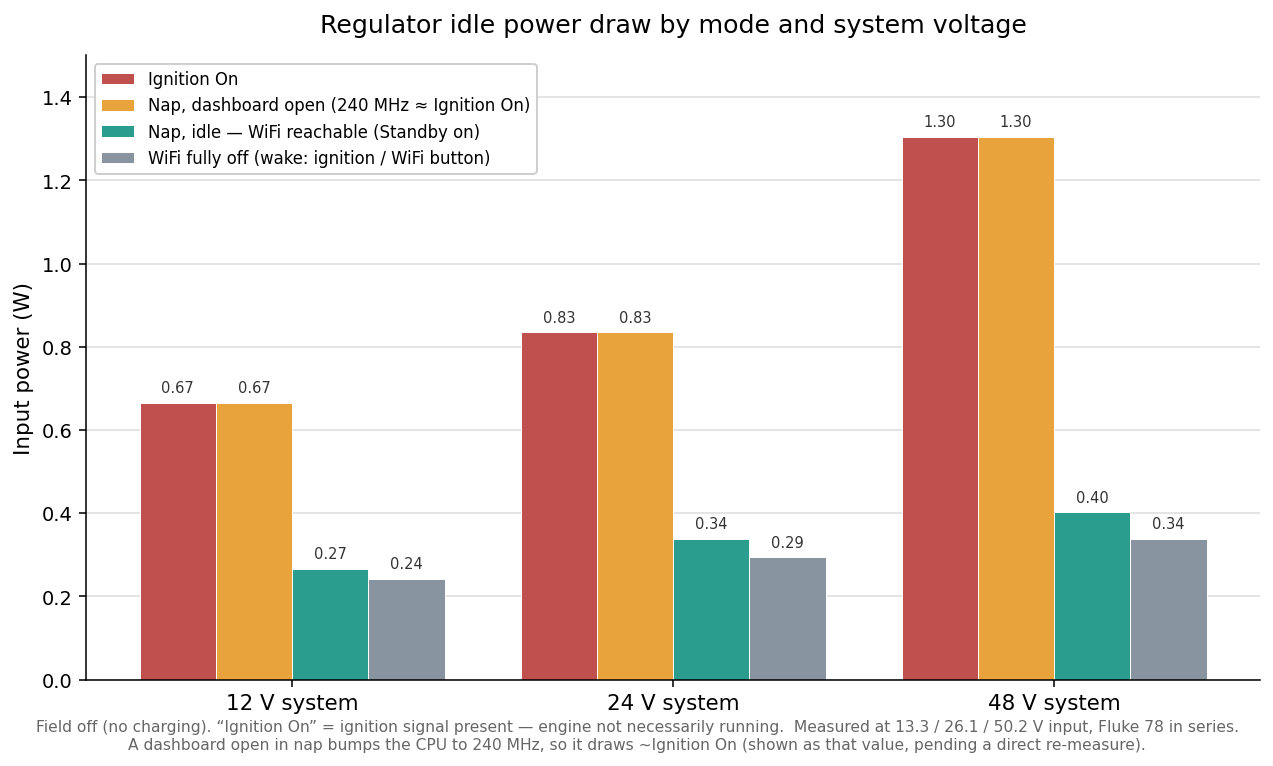
| Mode | 12 V system | 24 V system | 48 V system |
|---|---|---|---|
| (measured input) | 13.3 V | 26.1 V | 50.2 V |
| Ignition On | 50 mA · 0.67 W | 32 mA · 0.84 W | 26 mA · 1.31 W |
| Nap, dashboard open † | ≈ 50 mA · 0.67 W | ≈ 32 mA · 0.84 W | ≈ 26 mA · 1.31 W |
| Nap, idle, WiFi reachable (most common) | 20 mA · 0.27 W | 13 mA · 0.34 W | 8 mA · 0.40 W |
| WiFi fully off | 20 mA · 0.24 W | 12 mA · 0.29 W | 7 mA · 0.34 W |
† Nap, dashboard open runs the CPU at 240 MHz while a client is connected (for a responsive UI), so it draws essentially the Ignition On figures — a touch lower in practice, since the temperature task stays suspended in nap. The values shown are the Ignition On measurements as a stand-in; the earlier 80 MHz measurement of this state read 36 / 22 / 14 mA. Nap-idle (no client) is unaffected — it stays at 80 MHz, so the most-common row below is unchanged.
The WiFi-fully-off row was measured at 12.1 / 24.5 / 48.4 V. Note that nap-idle reads the same as WiFi-fully-off at every voltage — keeping WiFi reachable in nap costs only ~1 mA on average (WiFi wakes briefly for router beacons, peaking a few mA above the floor). Staying reachable on demand is effectively free.
Standby energy cost (Nap, idle — the most common state)¶
Assuming the regulator spends a full 24 h in nap-idle:
| System | Input | Idle current | Lost per 24 h | Energy per 24 h |
|---|---|---|---|---|
| 12 V | 13.3 V | 20 mA | 0.48 Ah | 6.4 Wh |
| 24 V | 26.1 V | 13 mA | 0.31 Ah | 8.1 Wh |
| 48 V | 50.2 V | 8 mA | 0.19 Ah | 9.6 Wh |
For scale, the 12 V case is about 0.1 % per day of a 400 Ah house bank — roughly 3.4 Ah over a week left unattended.
Amp-hours fall with system voltage, but watt-hours rise
Higher-voltage systems lose fewer amp-hours (simply I = P/V), yet slightly more watt-hours — the buck converter is a little less efficient stepping 48 V down than 12 V at this very light load. Both columns are correct; they just measure different things.
Sensor contribution¶
Adding the alternator current sensor and the DS18B20 temperature sensor raised the draw by ~4 mA at 12 V (~15 mA on the logic side) — consistent with a hall-effect current sensor's ~10 mA bias plus the DS18B20's ~1.5 mA. Sensor load is a small, fixed adder on top of the figures above.
The 5 V buck (LMR36510, 1 A) was sized for the largest intermittent load — the 250 mA buzzer — not this housekeeping draw. Even with the buzzer drawing its full 250 mA on top of the idle load, the 5 V stage stays under half its 1 A rating, so there is ample margin.
5V System Rail — Power Mux and Load Distribution¶
The system 5V rail is the output of a TPS2116DRL power multiplexer. The TPS2116 selects between two inputs — the LMR36510 output (battery-derived) and USB 5V — and routes the active source to the system 5V rail. Priority and switchover behavior are governed by the TPS2116's internal logic.
| TPS2116 Decoupling | Status |
|---|---|
| C_in (each input pin) | Not populated |
| C_out (system 5V output) | Not populated |
The USB-C 5V input has no bulk capacitance in the current design.
5V System Rail Loads¶
All devices below are supplied from the TPS2116 output (system 5V rail):
| Device | Function | Local Decoupling |
|---|---|---|
| TLV62569DBV | 3.3V buck converter | C22 (4.7 µF) + C23 (1 µF) at VIN |
| MT3608 | Boost converter for alternator gate driver (12V) | C42 (22 µF) at VIN |
| LM2907 | Frequency-to-voltage converter | 1 µF at pins 5/6 (COL/V+) |
| SN74LVC1T45 | 1-bit level shifter (5V side) | 1 µF at VCCA (pin 1) |
| TPS2553 | Load switch (buzzer control circuit) | 0.1 µF at VIN |
| FDN340P | P-channel MOSFET | None |
| BC847 | NPN transistor | None |
The MT3608 generates a 12V boost rail from the 5V system rail. This rail is used exclusively by the alternator field drive gate driver (LM5109A). Output decoupling: C43 + C63 (22 µF each — see Capacitor Specifications). Full circuit documentation: see alternator_field_drive.md, Block 2.
3.3V System Rail Loads¶
The 3.3V rail is the output of the TLV62569DBV step-down converter, fed from the 5V system rail.
| Device | Function | Local Decoupling |
|---|---|---|
| ESP32-S3 | Microcontroller | TBD |
| ADS1115 | 16-bit ADC | TBD |
| INA228 | Current/power monitor | TBD |
| BMP388 | Pressure/temperature sensor | TBD |
| TLV9154IDR | Quad op-amp | TBD |
- Bulk capacitor on 5V system rail (optional, conservative sizing): A shared 10 µF on the TPS2116 output would improve transient response for load steps from ESP32 WiFi activity. Adding bulk capacitance increases energy available during a fault event — size conservatively. 10 µF is sufficient; do not use 22 µF or larger.