Reworks Applied to V9
The schematic and the BOM show the V9 board as drawn and as ordered. Every V9 board differs from them in the five places below, applied by hand after assembly. The rest of this site describes the board as built; this page is the reconciliation against the drawing.
Input stage gate resistor
Change: R30 is fitted as 1 MΩ. The schematic shows 10 Ω.
R30 sets how fast the input protection controller (TPS48000-Q1) turns on its pass MOSFETs at power-up. At 1 MΩ the gate ramps up over about a millisecond, so the board's protected rail rises without exciting the input filter's LC resonance. That keeps the turn-on overshoot small at every system voltage, including 48 V. Fault turn-off is unchanged: the controller pulls the gate down through a separate direct path, so R30 plays no part in how quickly the board isolates on an overvoltage trip. Circuit context is in Input Protection.
1-Wire pull-up
Change: R77 is fitted as 1.0 kΩ, 1 %, 1 W, 2512 (YAGEO RC2512FK-071KL). The schematic shows 4.7 kΩ.
R77 pulls the DS18B20 data line up to 3.3 V. The lower value makes the line rise faster against cable capacitance, so the temperature probes can sit at the end of long runs: about 260 ft on Cat5e or Cat6, or about 90 ft on shielded 3-core cable, with margin. The value keeps the sensor at 73 % of its rated sink current, so both low levels stay inside specification. Details are in Temperature Sensors.
Fast alternator-current tap
Change: C66 not fitted. A jumper from the alternator-current buffer output (U9 pins 6 and 7) to J3 pin 11, which lands on ESP32 GPIO3.
The buffered alternator-current signal feeds two converters. The ADS1115 reads it for charge control; the tap gives the ESP32's own ADC a copy of the same signal, sampled at tens of kilosamples per second. The disturbance-analysis features (the ripple map, rectifier fault detection, and the live waveform view) run on this channel. Leaving C66 out keeps the 1 µF filter off the tapped node, so the full signal bandwidth reaches the ESP32 without loading the buffer that feeds the control path. Details are in Analog Inputs.
Field return diode and crowbar
Change:
- D8 not fitted.
- Return diode added, SB5H100 (Vishay, 100 V 5 A Schottky): anode on FIELD_FOR_N_TYPE, cathode on the BAT+ input.
- Crowbar diode added, 10A10: anode on GND, cathode on the BAT+ input.
The return diode carries the field winding's current whenever the field MOSFET (Q3) is off in N-type wiring. It lands on the battery side of the input protection stage, so the freewheel loop, through the diode, the Regulator BAT+ wire, and the alternator output cable, stays intact whether the protection stage is conducting or has tripped. A protection trip with the field energized is then a clean shutdown: the field energy decays in the winding and the diode, and no board node rises above battery voltage. No external clamp module is needed for N-type installations.
Without D8, the board's own rail is fed only through the input protection stage in both wiring types, so an overvoltage trip fully isolates the board.
The crowbar diode makes a reversed battery connection clear the BAT+ fuse directly, through a single diode, rather than through the field output stage. It is idle at all other times.
The three changes are a set. Without D8, the return diode is the only freewheel path for N-type wiring, so neither added diode may be removed. In P-type wiring the return diode sits across the terminal 1 to terminal 3 bridge and has no effect on operation; the crowbar protects both wiring types.
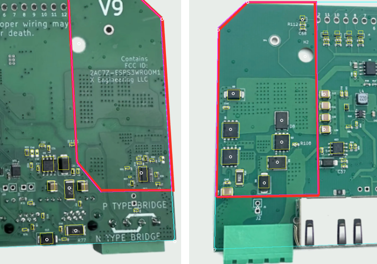
D5 heat spreader
Change: Graphite heat-spreader film added around D5, one layer on each face of the board: Würth Elektronik WE-TGS, part number 4051100100017.
The film keeps D5, the field freewheel diode, cool in high-voltage installations. The red outlines show its coverage on the back of the board (left) and the front (right).